~vibrato/chorus~
video demo - coming soon
a typical chorus effect splits the input signal into two paths. one path is frequency modulated to some degree, then combined with the original "dry" signal. depending on the intensity and rate of the modulation, many different sounds can be made using this technique, this can be seen on Figure 1. i had a Boss CH-1 pedal (analog chorus pedal using a BBD delayline) that i really enjoyed the sound of. i applied a popular modification to it that removed the dry signal, leaving only the pitch modulated signal path. i really liked the sound of the frequency modulation, but was left wanting more control. i decided to design my own chorus/vibrato effect with complete control over the frequency modulation and mixing of the modulated and dry signals.

fig. 1 - both signals (red), frequency modulated signal (blue), dry signal (green)
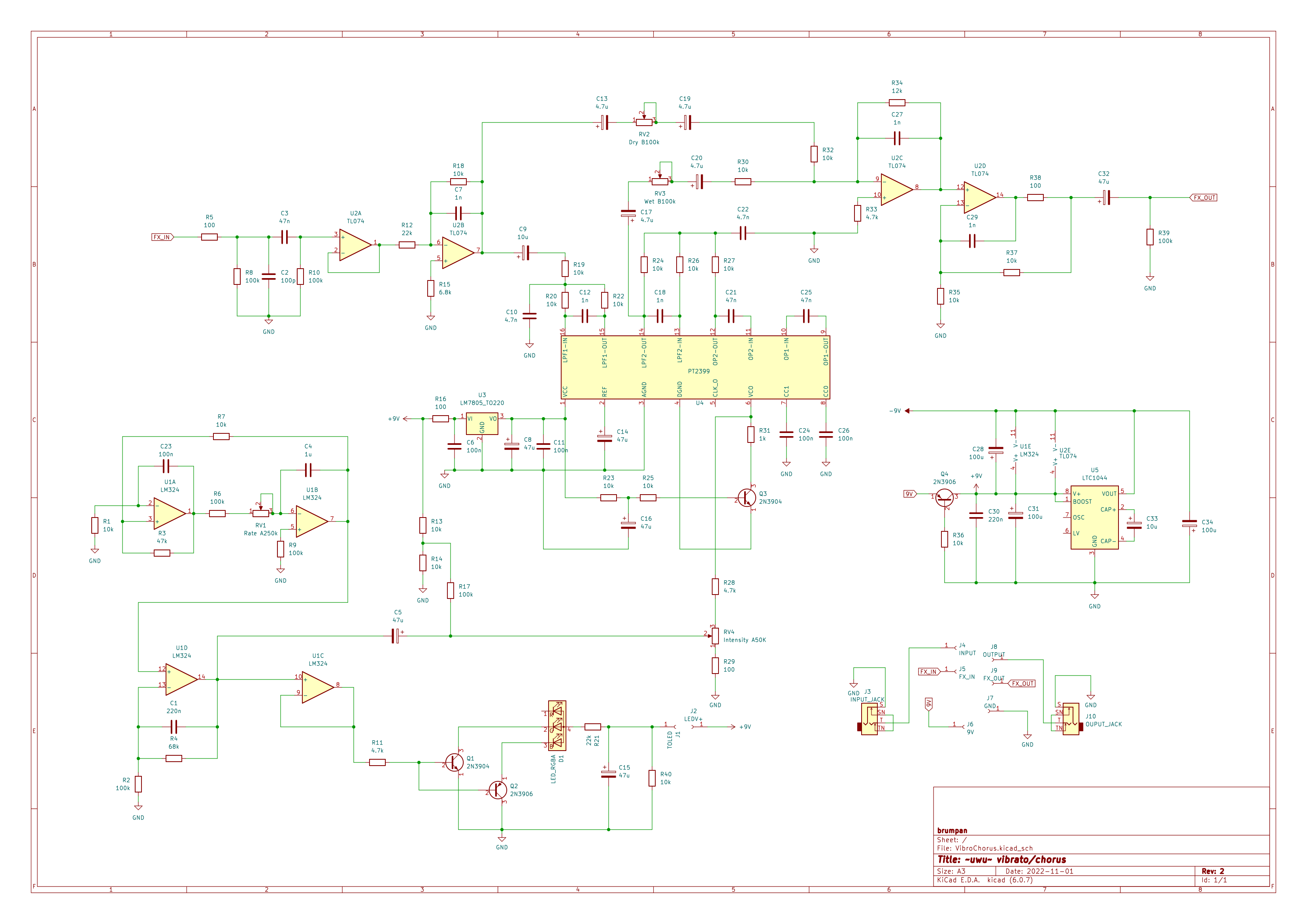
due to the insane prices of BBD delay chips i decided to use a PT2399 delay IC. these chips are still in production and are relatively inexpensive. there are many helpful tutorials on how to work with these ICs (the datasheet that is provided by the manufacturer is not very helpful), i found electrosmash and ESP had the most helpful information on designing circuits with these ICs. the basic principle of the design is similar to conventional chorus designs. the input signal is split, one channel is sent through the delay line. the delay line time is changed using an external LFO where the rate is variable from around 2-10Hz. the intensity at which the delay line's time changes is also variable. the delay line is set to its minimum value using a transistor timing circuit, this allows the PT2399 to perform frequency modulation to the signal with minimum latency (around 40ms).

fig. 2 - schematic (click for hi-res)
i have also implemented an TC1044S switching regulator to provide a -9V supply rail for the TL074 and LM324 op amps. the recommended minimum operating voltage for the TL074 is between ±5V and ±15V, and with this switching regulator i was able to provide ±9V which is well within the nominal value. the switching regulator operates at a frequency of around 45kHz when the "boost" pin is connected to Vcc, which was well outside the audio range.
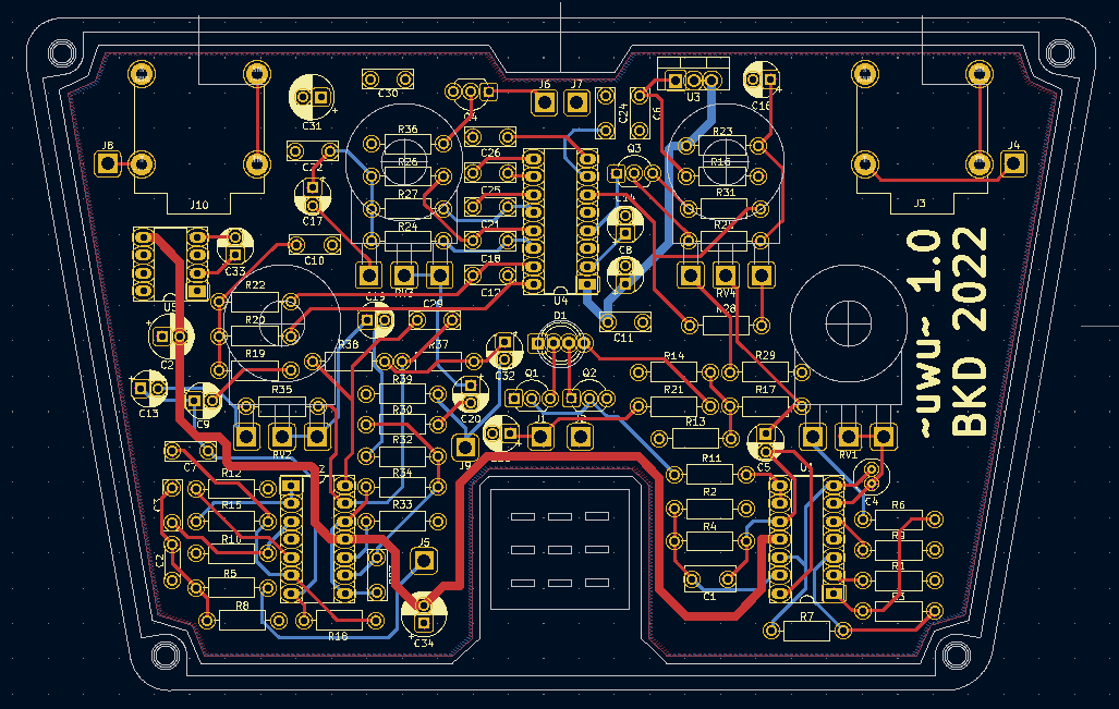
the circuit is very quiet, on the layout i isolated the LFO from the signal paths by placing them on opposite sides of the board and providing a large capacitor between the supply rails. during my first prototype of the project there was some loud popping noise from the LFO, due to the rail-to-rail square wave section of the oscillator. i was able to remove the noise by adding C23, which acts as an integrator, getting rid of the high-frequency cmopnents of the square wave section of the oscillator.

fig. 3 - original pcb design in KiCad

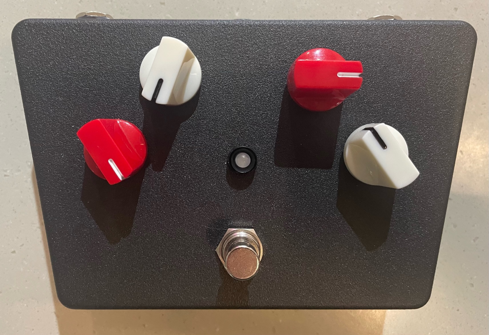
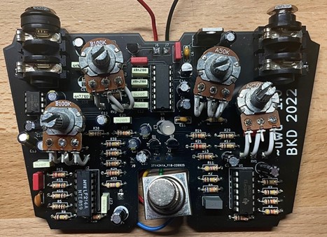
fig. 5 - finished unit in enclosure
this project turned out exactly how i wanted it to. the effect can produce some really subtle tape-like chorus and wobble effects, or sound like a crazy laser gun. in the future i will likely condese this schematic into a smaller enclosure using smd components on both the top and bottom of the board. i would also like to add a waveform selector for the LFO.
