~pv current sensor~
video demo - coming soon
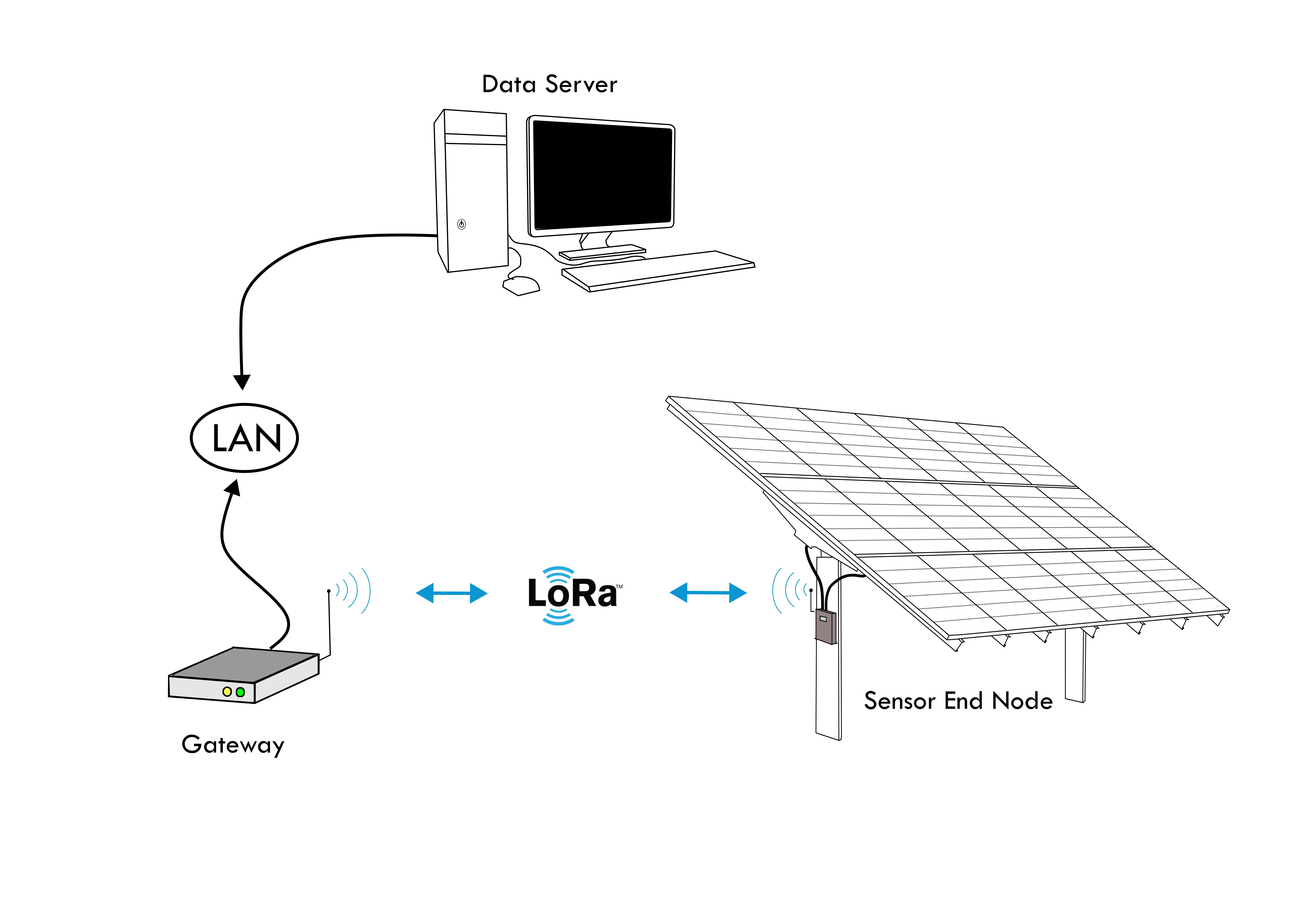
for my senior project i teamed up with another student to design a sensoring application for photovoltaic panels in microgrid systems. our systems uses a current sensing end node and transmits data over the lorawan protocol back to a chirpstack server where the data can be viewed and informed decisions about the system. lorawan utilizes the lora communication protocol created by semtech. lora is a low-bandwidth, low-power, and long distance radio that operates on the 915MHz frequency band (in the US).
the end node was my responsibility. the first thing i did when setting out to develop the node was gather a list of features I thought the node should have. I determined the node should have the following:
○ in-line current sensing up to 50A ○
○ lora communication ○
○ battery power supply ○
○ capable microcontroller ○
○ visual display ○
○ environment sensor ○
○ manual controls ○
in addition to these features i also wanted the module to be able to take power either directly from the pv lines, from its own small solar panel, or via usb.
for the current sensing device I chose the TLI4971-A075T5 hall-effect AC-DC current sensor module. it has an extremely low resistance of 220µΩ across the terminals, up to 75A of current through the sensing terminals, and over-current protection. for lora communication i chose the hopeRF RFM95. this lora module operates at the 915MHz frequency and there is ample library support for arduino. at first i had planned on using a typical AVR microcontroller like the AtmegaU32, but at the time that i was selecting components there was a shortage for these parts. instead i decided to use the raspberry pi pico microcontroller, the rp2040, which was in stock across most vendors. this microcontroller is capable of being programmed in arduino/C++, and a stripped down version of python called micropython. the remaining peripherals and features are less interesting and are basic implementations based on their datasheets.
with the features decided upon, i set out to find components that would allow the node to provide all the features. after sourcing components, i moved to the schematic phase.

fig. 1 - schematic diagram
once the schematic was designed a layout was created in kicad. the pcb was designed to fit a nema 4x enclosure with a clear cover. the current sensing side of the board is thermally isolated from the rest of the board, this also protects the main board from any mechanical strain from attaching the pv lines.

fig. 2 - pcb layout
pcbs currently being manufactured at jlcpcb - 4/14/23